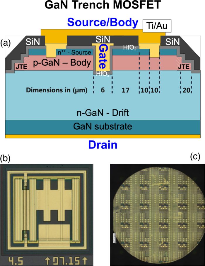
Next-generation power electronics are leveraging the advantages of wide bandgap semiconductors to enable higher power densities and efficiency. In electric vehicle drivetrains, this translates to lighter weight systems and more miles per charge. Vertical gallium nitride (GaN) power devices promise a similar advantage as silicon carbide (SiC) by leveraging a large breakdown electric field. However, for 1200 volt applications and below where channel resistance dominates, the addition of compatibility with a high-κ gate dielectric can provide significant performance advantage for GaN over SiC.
Sandia National Laboratories has demonstrated GaN-based 1.2 kV MOSFETs with a first-of-its-kind integration of a hafnium dioxide (HfO2) gate dielectric. Until now, the use of a HfO2 high-κ gate dielectric was thought to be incompatible with wide bandgap semiconductors due to high leakage and low band offset. Sandia’s process has not only achieved record low gate leakage but also demonstrated an order of magnitude improvement in on-state current densities compared to reports from state-of-the-art GaN and SiC devices. The results from this work attest that high-κ gate dielectrics are useful and viable for improving current density and performance for wide bandgap semiconductors.
This research was conducted as part of the Electric Drivetrain Consortium, sponsored by the DOE Vehicle Technologies Office.
December 23, 2024